In recent years, GaN-based light-emitting diode (LED) have been widely recognized to be the most promising alternative light source for general lighting.1,2) Using the break through patterned sapphire substrate technique, Nichia Corporation has achieved high-brightness GaN-based LEDs with a record-high efficiency of 150 lm/W.3,4) The enhancement in efficiency of GaN-based LEDs on patterned sapphire substrates is generally attributed to the improvement in both light extraction efficiency and internal quantum efficiency.5–9) The improvement in internal quantum efficiency is due to the reduction in threading dislocation density by the achievement of lateral growth of a GaN epilayer on the patterned sapphire substrate.10–13) The light extraction efficiency is enhanced by the regular pattern created on the sapphire substrate, which counteracts the effect of total internal reflection (TIR) at the GaN/sapphire interface.5)
Numerous patterning features produced on patterned sapphire substrates by either dry etching or wet etching sapphire, which include circular cavities, square cavities, hemispherical bumps, and trenched stripes, have been studied.5,14–17) However, no matter what etching process is used to create the patterns, a hard-mask (SiO2 in most cases) lithographic process is required on the flat c-plane sapphire wafer. In this study, we utilize a mask-free wet-etching process to produce a so-called nature-patterned sapphire substrate (n-pss), with a unique pyramidal pattern on the c- plane sapphire surface. In addition, metal organic chemical vapor deposition (MOCVD) is used to grow a GaN epitaxial layer with an LED structure on the n-pss wafer. The optical and electrical properties of horizontal LED chips fabricated on the n-pss wafer are characterized in detail.
The mask-free wet-etching process used to produce the pyramidal n-pss wafers is described in detail in the following. Before the wet etching process, a SiO2 layer was deposited by plasma-enhanced chemical vapor deposition (PECVD) on the back side of the c-plane sapphire wafer to prevent the back side from being etched. The flat back side of the patterned sapphire wafer also enables good contact with the bottom of the growth pot in the MOCVD chamber, which ensures the high quality of the MOCVD epitaxial process. After deposition of the SiO2 back side layer, the sapphire wafer was immersed in pure H2SO4 . The etching temperature was controlled at a constant temperature of 320 ‘C for periods of 15, 30, and 60 min. After etching, dilute HF solution was used to remove the SiO2 back-side layer. Finally, the etched sapphire wafer was successively cleaned by acetone, isopropyl alcohol (IPA), and distilled water (DI water).
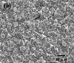
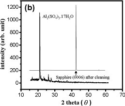
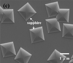
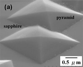
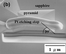
We found that H2SO4 did not significantly etch the sapphire wafer in the thickness direction. Instead, it was found that a massive cubic etching product phase completely covered the surface of the sapphire wafer, as shown in Fig. 1(a). X-ray diffraction (XRD) was used to identify the exact compound phase of the etching-product. As shown in Fig. 1(b), only one strong peak appears in the XRD diffraction pattern, which matches the standard XRD diffraction pattern of the Al2(SO4)3-17H2O phase. Dwikusuma et al. also reported similar findings, i.e., the formation of the Al2(SO4)3-17H2O phase on sapphire etched by H2SO4. 18) However, Dwikusuma et al.’s XRD result showed all the diffraction peaks of the Al2(SO4)3-17H2O phase but in the present study, the Al2(SO4)3-17H2O etching product exhibits an orientation-preferred XRD diffraction pattern. Faceted pyramids were observed on the n-pss wafers after removal of the etching product in dilute HCl solution. Figure 1(c) shows an enlarged scanning electron microscope (SEM) image of the facet pyramids on the n-pss wafer surface. We found the size of the pyramids on the n-pss wafer to be reasonably uniform, the height and width of the pyramids being about 0.2 and 1.5 mm, respectively. In addition, a flat c-plane sapphire surface appears between the pyramids. This flat c-plane sapphire surface is of importance since it can provide suitable nucleation sites for the initial growth of the buffer GaN epilayer on the patterned sapphire substrate. The average coverage percentage of the pyramids on the etched sapphire wafer is about 44%. Note that patterns typically cover about 50 to 70% of patterned sapphire substrates.5,15,17) In other words, the percentage coverage of the currently studied pyramidal pattern on the etched sapphire wafer is less than the typical coverage.

